Index of /muonsortes

a dev log // last updated 2026-05-20

project Muon Sortes

what A desk clock that consults the sky. Four Geiger-Müller tubes watch for cosmic ray muons passing through pairs simultaneously. Each coincidence draws a lot. The lot becomes a decision, a digit, a tick.

stage Breadboard. Tubes counting, coincidence circuit under debug, enclosure in design.

photos No AI renders here. Real photos as the build happens — poorly lit breadboards now, prototypes when they exist.

name "Sortes" is Latin — the lots Romans drew to ask the gods a question. Now drawn by particles older than the planet.

also at hackaday.io/project/205541

mailing-list.txt
One email when the device exists. One when it ships. That's the list.
/log

From e-ink headaches to high voltage unknowns

It's been a few weeks since the last update and a lot has happened, so this is going to be a longer one covering multiple milestones. I'll try to keep it moving.

The display swap

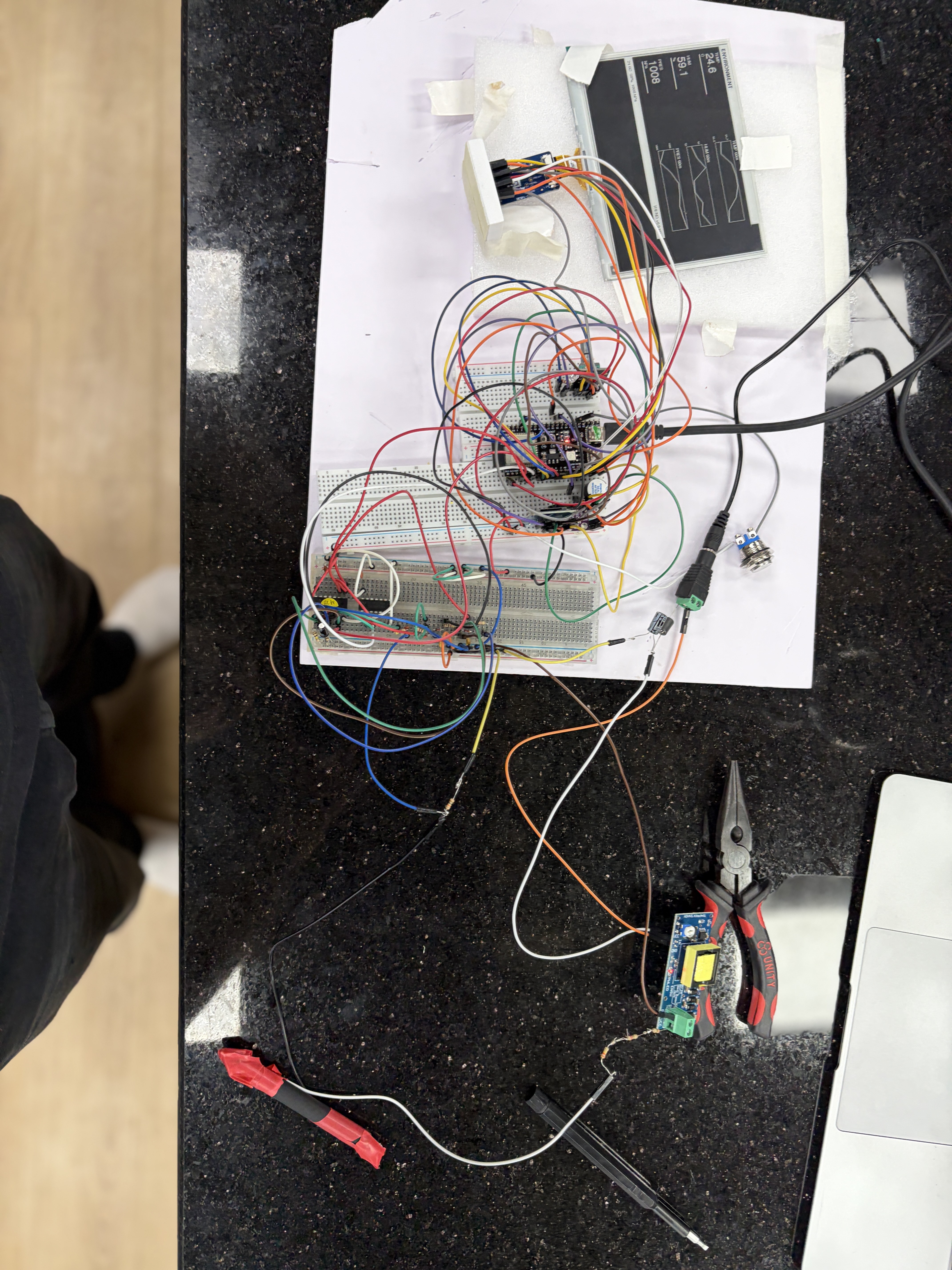
While waiting for the HV boost modules I started working on the e-ink display. I'd originally planned to use a Waveshare 3.97" (800×480, 4-level grayscale) but switched to a Good Display 5.79" wide-format panel (792×272, monochrome) because it had a much faster full refresh on paper (3.5s v 0.7s). Trade-off is losing grayscale, but for a clock and oracle readout, monochrome with good typography is plenty.

What I didn't expect was spending a full week debugging this thing. I've realized it doesn't do partial updates without RAM buffering, I just assumed it had partial updates, and my little ESP32 is just barely enough, so to avoid this again, I just went and ordered an e-reader HD display and we are going to call it a luxury experience. I'll go more into it later, I've put the display on the back burner now that the HV boosters have arrived.

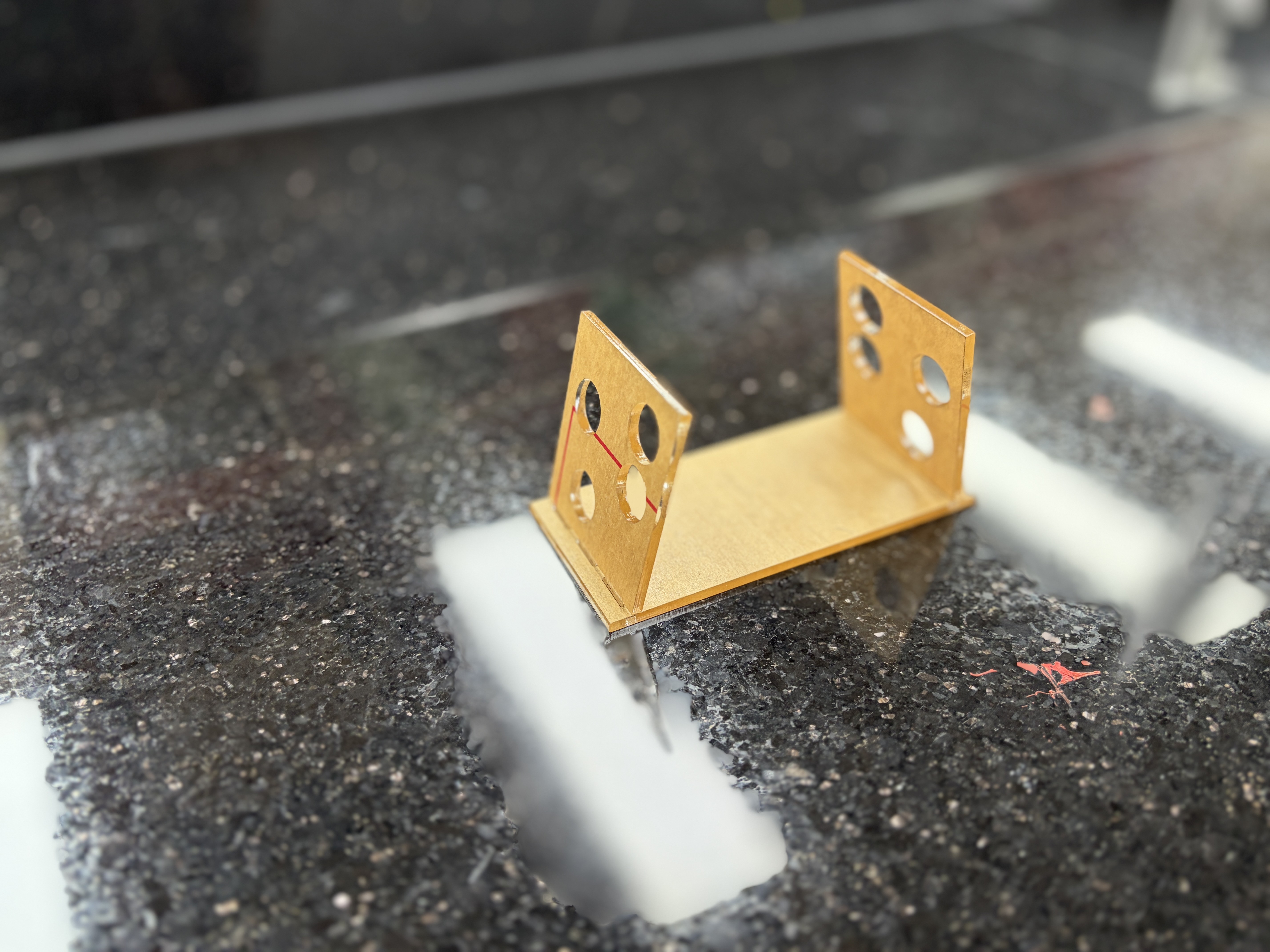
Laser-cut tube scaffold

I had an acrylic scaffold laser-cut to hold four J305 tubes for testing. The design puts each of the six possible tube pairs at a different angle with a different geometric aperture, so I can eventually compare coincidence rates across different alignments. The tubes are wrapped in black heat shrink for light shielding (J305s are photosensitive and will false-trigger from ambient light), then taped securely into the cradles.

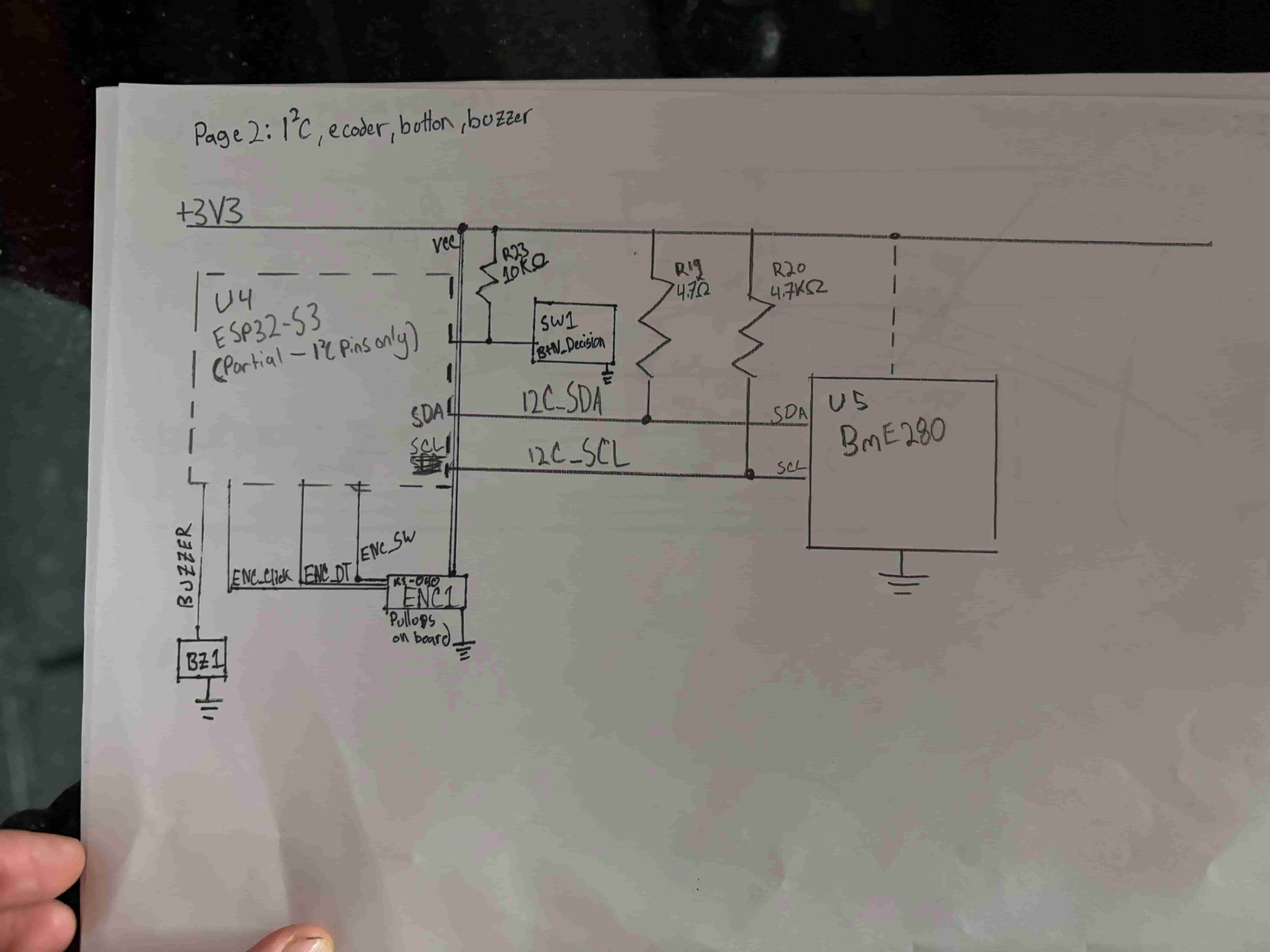
Single tube bring-up

The HV boost modules finally arrived and I spent a full day getting a single tube working. It did not go smoothly.

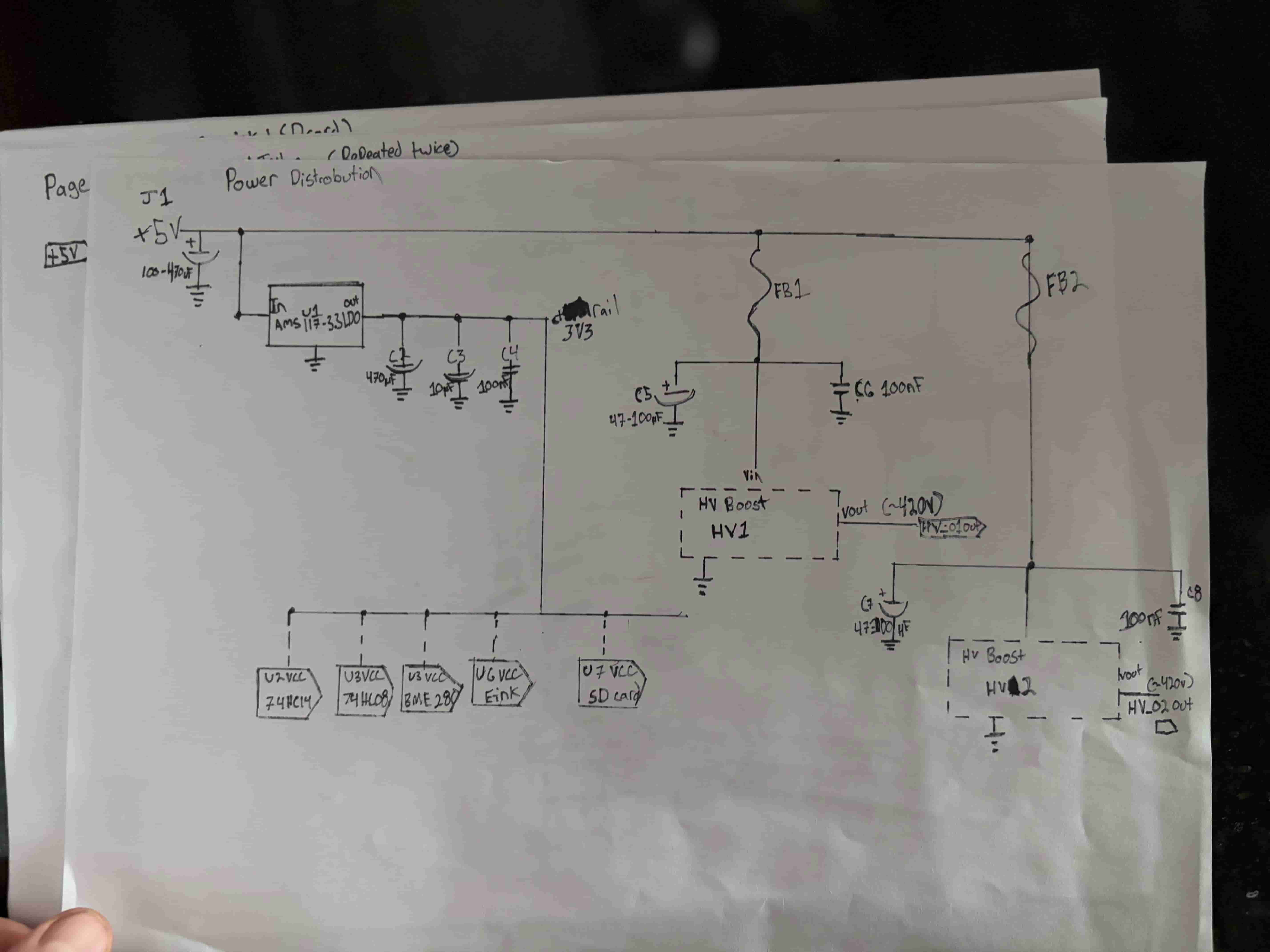
First problem: one of the HV boosters was dead on arrival. No output at all, trimpot did nothing. Swapped it for the second module and got a clean ~410V output. Good reminder to always order spares — I have more on the way.

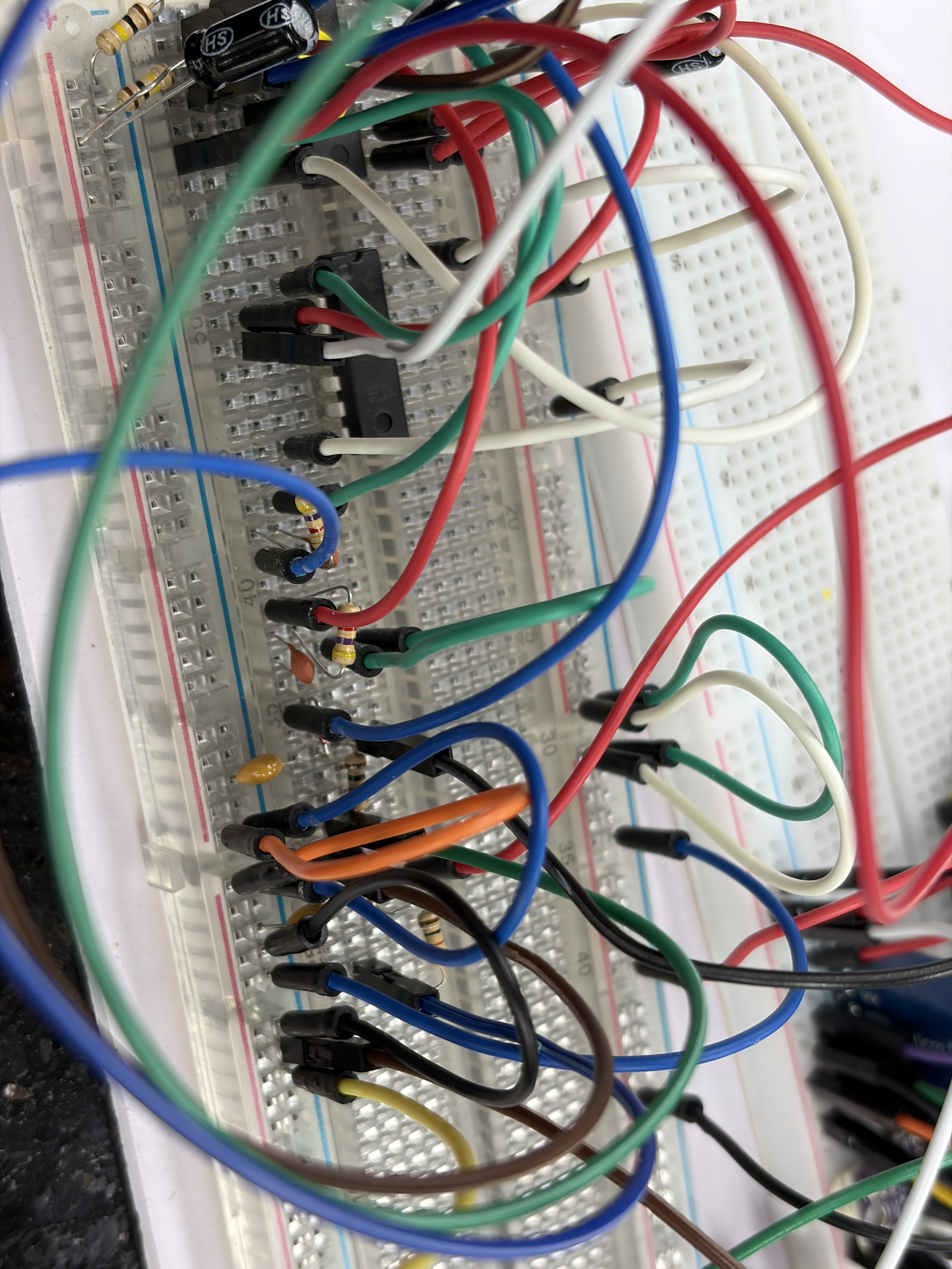
Second problem, and the one that ate most of the day: with a working HV module and a tube connected, I was getting zero signal. The tube was powered, presumably counting background radiation, but nothing was making it through to the ESP32. I went through the chain methodically — checked voltages, checked connections, then checked the 74HC14 inputs — and eventually traced it to the pulse stretcher. The BAT54/RC network that worked perfectly with clean synthetic pulses from the ESP32 wasn't behaving the same way with the real analog signal from the cathode. I rebuilt the stretcher section and it started working. I probably had a jumper out of place.

That moment when the serial monitor starts printing counts at roughly the right background rate (~25–40 CPM for a J305) is genuinely satisfying. Finally one tube, clicking away, counting background radiation on my desk in Hanoi.
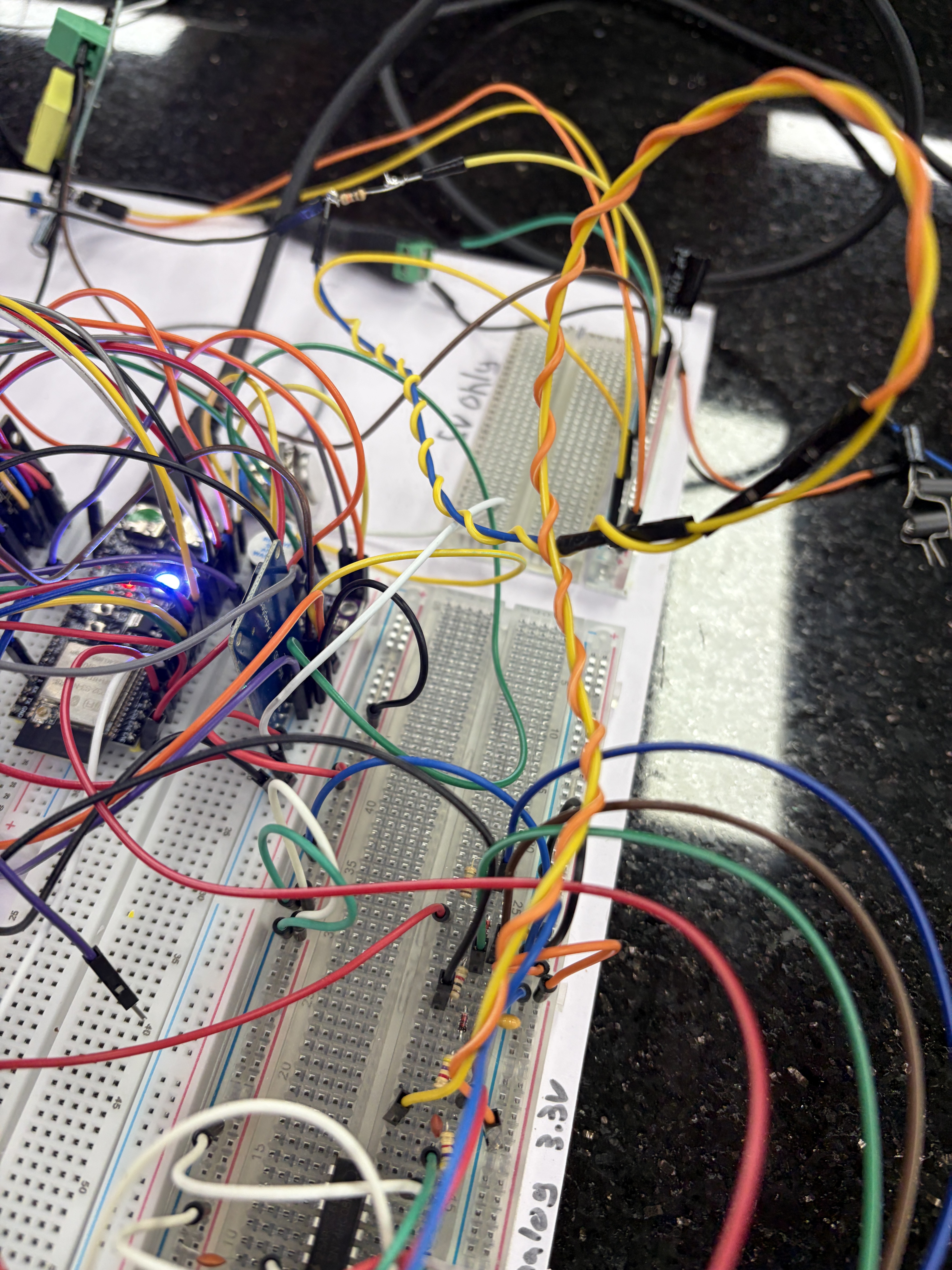
Two tube rebuild

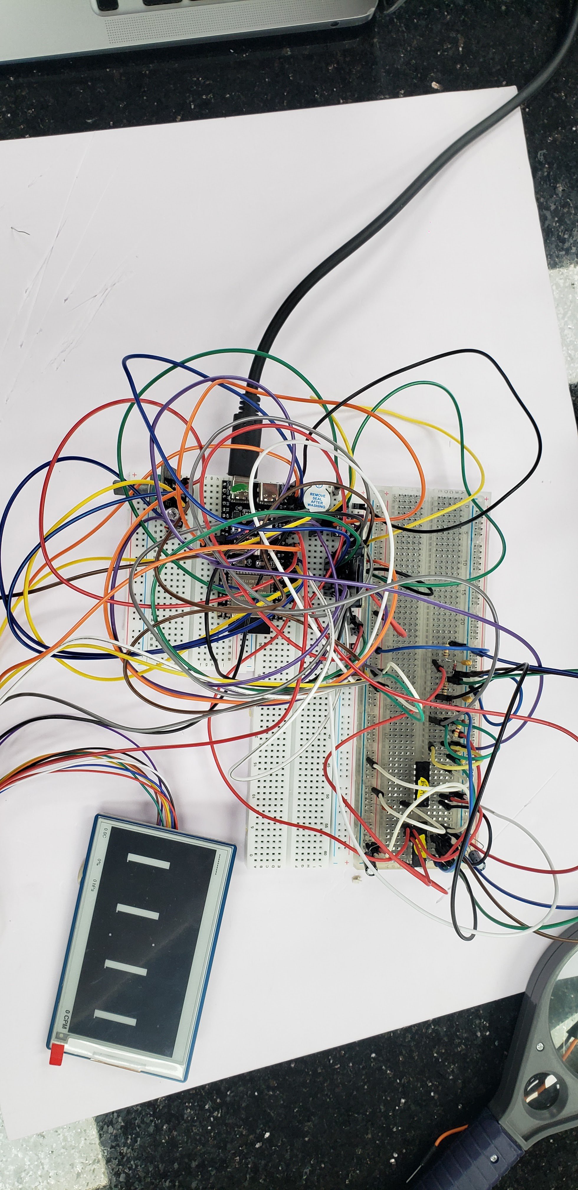
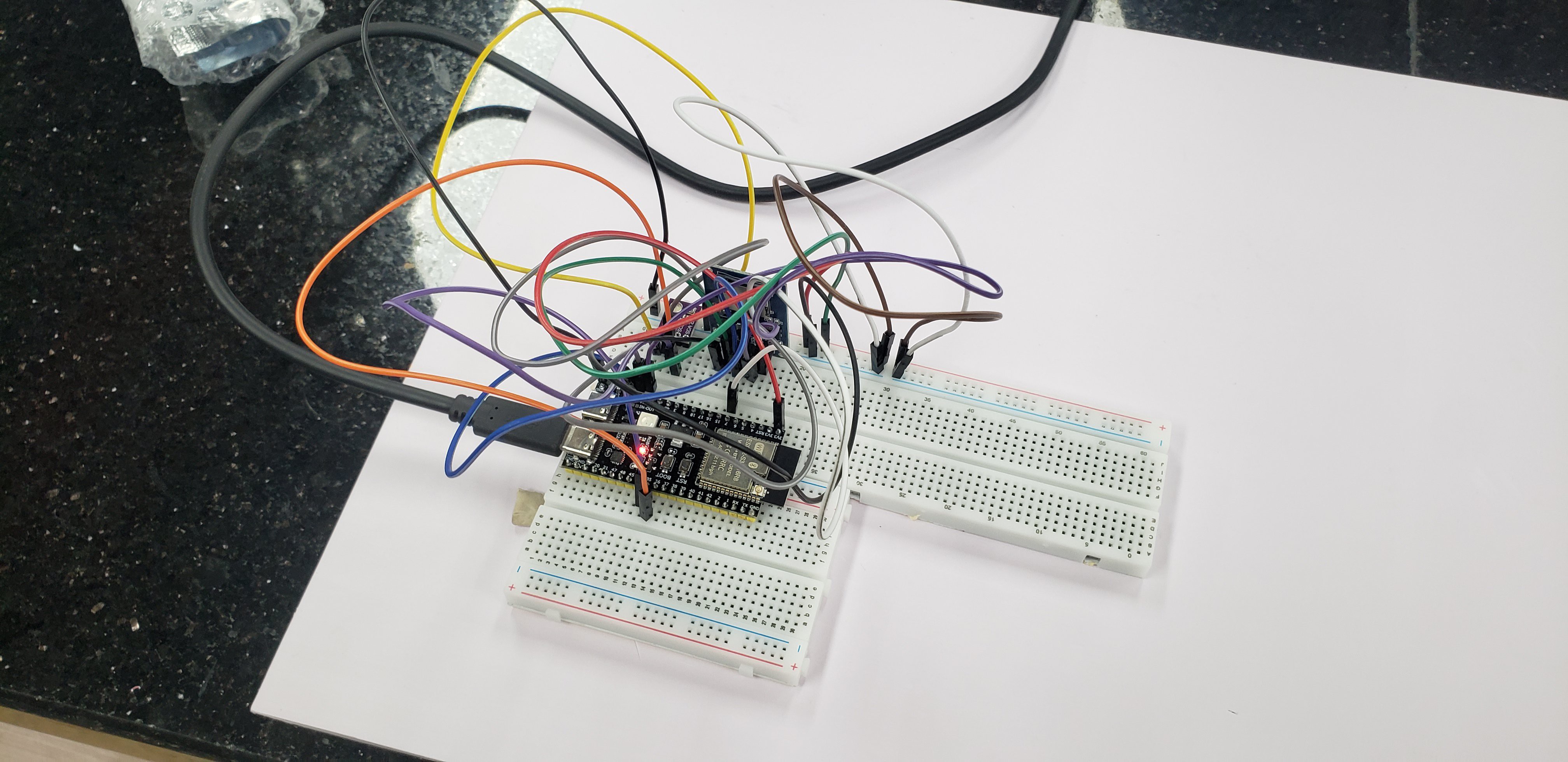
With one tube proven, I broke down the single-tube setup and rebuilt for two channels. This is where it got messy.

The second channel needed its own pulse conditioning chain — coupling cap, bias network, 74HC14 shaping, stretcher, re-squaring — a copy of the first one. And the coincidence gate needed both stretched outputs feeding the 74HC08 AND gate cleanly. In theory I'd already validated all of this with synthetic pulses. In practice, with real analog signals and two HV modules running simultaneously, new problems appeared.

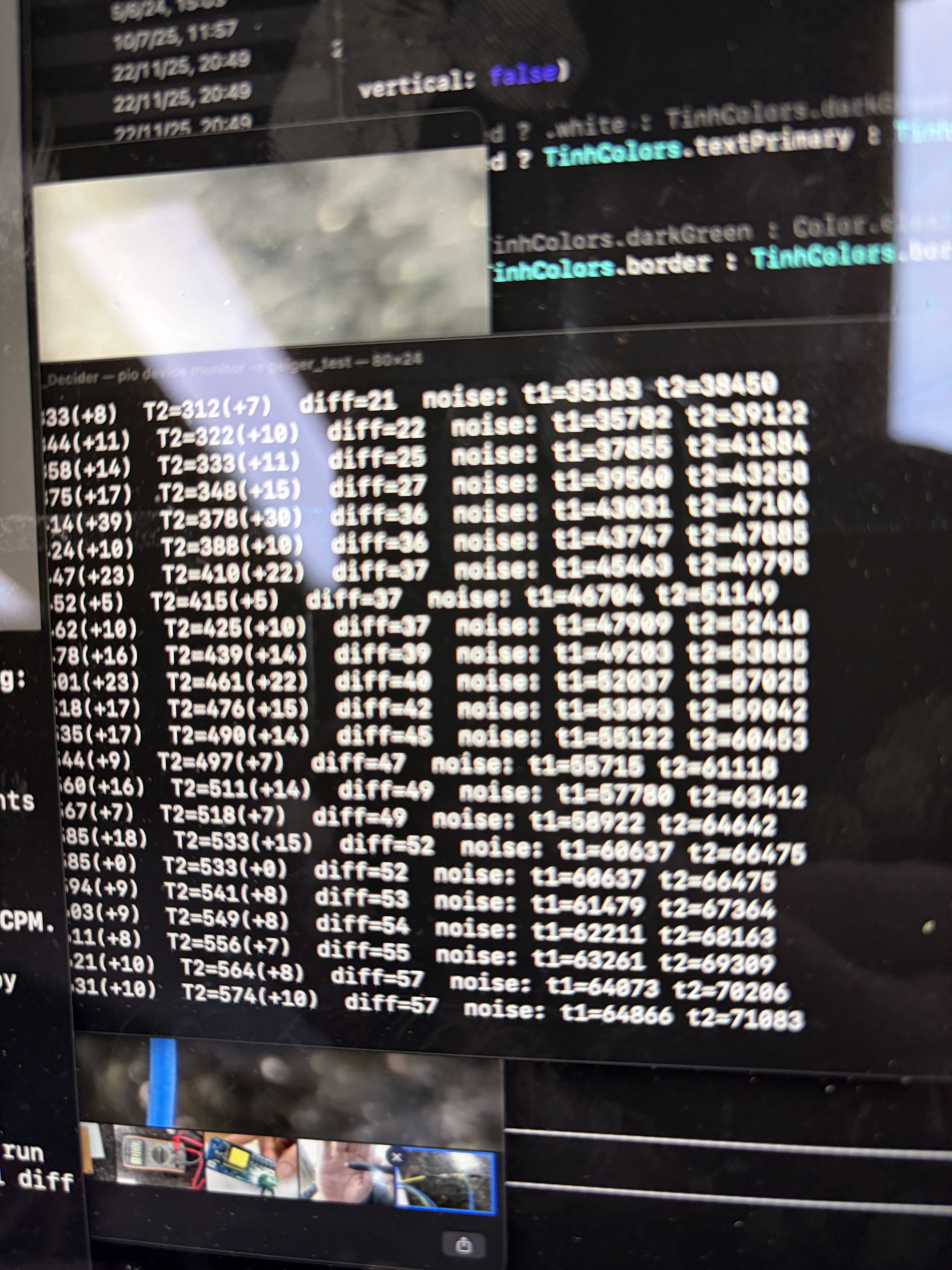
The coincidence timing was off. I was either getting zero coincidences (window too narrow or pulses not overlapping) or suspiciously high counts that were clearly noise rather than real events. First I was getting 1000+ hits a second — clearly noise. I wrapped the cathode lines with grounded cables, that brought it down to 200-ish.

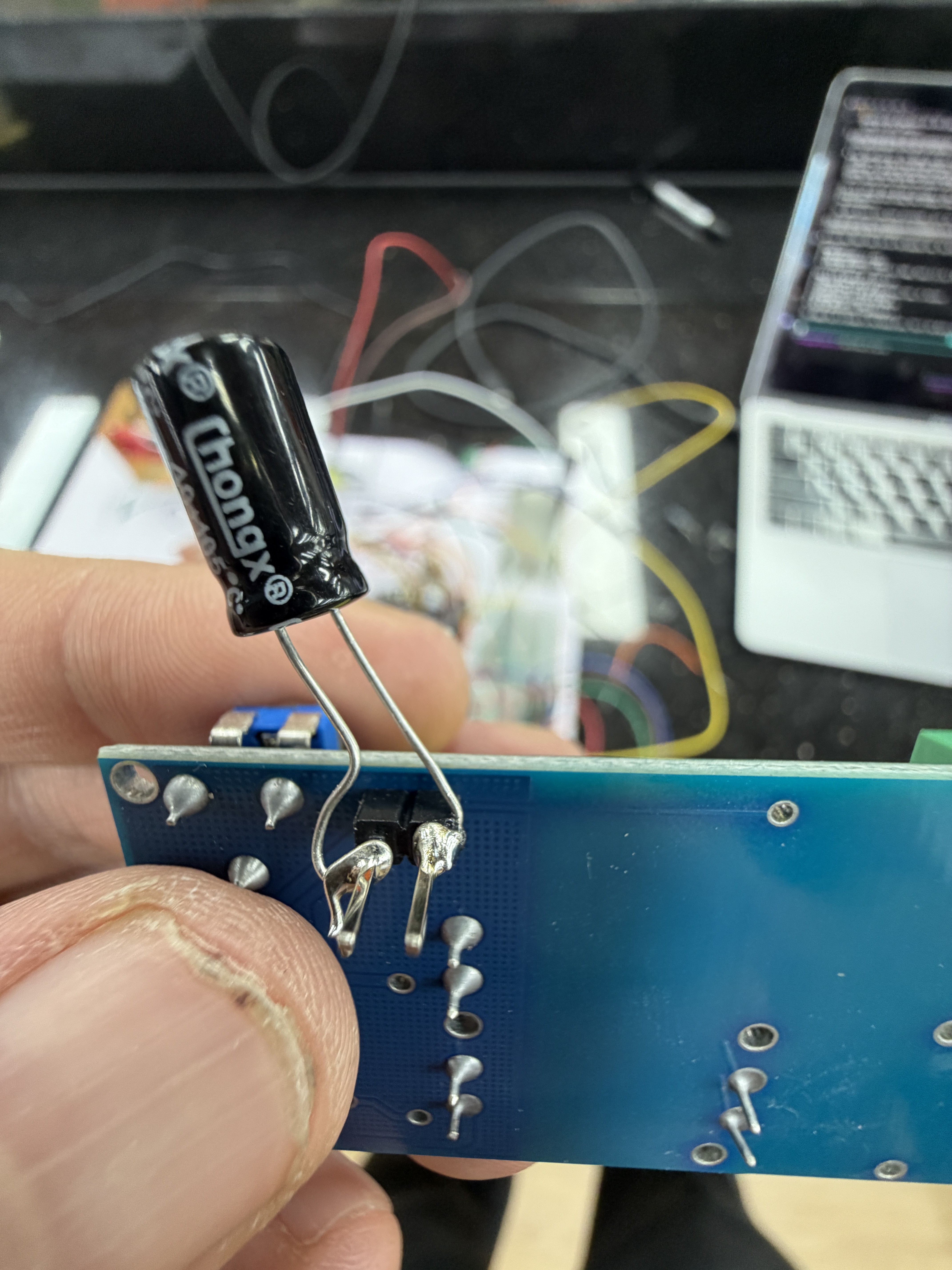
Then I threw capacitors on the HV boosters' inputs (which felt so wrong). That brought it down to around 30. I tried to solder up a tiny 100pF ceramic cap and it was a joke, didn't do anything. Interestingly enough, Claude recommended ferrite beads on the input...

Testing the signal chain with synthetic pulses

Before the HV boost modules arrive (40 days in transit), I wanted to validate as much of the detection circuit as possible using just the ESP32 itself. The idea is simple: use one GPIO as a signal generator to inject fake pulses into the front end, and use another GPIO to listen for interrupts at the output. If the right number of pulses come out the other end with the right timing, the chain works.

Digital chain first

I started with just the digital side — the 74HC14 pulse shaping, BAT54/RC stretcher, second 74HC14 re-squaring stage, and the 74HC08 AND gate. I wrote a quick sketch that toggles a GPIO to produce short pulses at a known rate, fed those into the 74HC14 input, and counted rising-edge interrupts on the AND gate output with a separate pin.

For single-channel testing I injected pulses into one channel at a time and confirmed the ESP32 counted every one. For coincidence testing I fed the same pulse into both channels simultaneously. The AND gate output fired on every injected pulse, which is exactly what you'd expect when both inputs see the same signal at the same time. I also confirmed that pulsing only one channel produced zero coincidence counts on the output. That's the whole point of the AND gate and it's reassuring to see it actually reject single-channel events.

Not the most sophisticated test — a logic analyzer would let me see the actual pulse shapes at each stage and verify the stretcher timing. But for a go/no-go check of "is this circuit wired correctly and are the ICs behaving," it's enough. The logic analyzer is sitting on my desk for when I need it later.

Then the analog front-end

With the digital chain proven, I wired up the analog input network: the 1nF coupling caps, 4.7kΩ series protection resistors, and 100kΩ bias pull-downs that sit between the GM tube cathodes and the 74HC14 inputs. No tubes, no HV, just the passive components that will eventually condition the real cathode pulse.

Same test: synthetic pulses from the ESP32 into the analog input side, interrupt counting on the coincidence output. The pulses now travel through the full path — coupling cap, bias network, first Schmitt trigger stage, stretcher, re-squaring, AND gate. Everything that isn't the tube and HV module.

It worked. Same pulse counts in, same counts out. The coupling caps and bias resistors aren't filtering out or attenuating the synthetic pulses, which makes sense because the ESP32 GPIO puts out a clean 3.3V edge that's well above the 74HC14's ~1.9V threshold. The real question is whether actual GM tube cathode pulses will be strong enough, and that's something I genuinely won't know until the HV modules show up and I can power a tube.

That's the next milestone: HV module bring-up. The boost converters are still in transit, so in the meantime I've been working on the e-ink display, which turned into its own adventure. More on that next time.

Digital circuits breadboarded

With the schematics drawn and parts sorted into their labeled bins, it was finally time to start populating a breadboard. The plan was to build the entire digital chain first — pulse shaping, stretching, re-squaring, and the coincidence AND gate. Without any of the analog front-end, and definitely without any HV anywhere on the bench.

I'll spoil the post: it was uneventful. Which is the goal, honestly. The fun part of breadboard work is that satisfying click of components going into rows and the slow accumulation of a circuit that starts to look like the schematic on paper. Two 74HC14s, a 74HC08, a 100nF decoupling cap on every IC's VCC pin (every IC!!), the BAT54 diodes and RC networks for the stretchers, all the bias and pull-down resistors. About an hour of work, a couple of moments where I had to recount pin numbers, and a finished chain.

A few small choices worth calling out:

The BAT54s are SOT-23 SMD parts, which is annoying on a breadboard. I soldered short lead wires onto each one before plugging them in. Ugly but functional, and they'll be replaced with through-hole packages once the design moves to PCB anyway.

I tied all unused 74HC14 and 74HC08 inputs to ground rather than leaving them floating. CMOS inputs that float pick up noise and can self-oscillate, which is exactly the kind of subtle problem you don't want chasing later when the analog side is also misbehaving.

I left the cathode pulse inputs (TUBE1_RAW and TUBE2_RAW on the schematic) terminated at unused breadboard rows for now. Those will get connected to the GM tubes once the analog front-end exists. Until then, they're just landing pads waiting for a signal.

Next post is going to be the more interesting one: validating that the chain actually works using synthetic pulse injection. I'm generating test pulses from an ESP32 GPIO and walking through the chain stage-by-stage with a logic analyzer to make sure each transformation happens the way the schematic says it should. That's the post where I find out if I drew the circuit correctly.

Designing a cosmic ray decision oracle on paper

I have been thinking about building a muon-based RNG device ever since watching an Alpha Phoenix video on YouTube. It seemed like such a cool way to have a direct connection to both sub-atomic and astronomical scales. I mulled the idea around for ~2 years and finally decided to pull the trigger.

I haven't designed a circuit from scratch since high school, but I have done a number of repairs on analog equipment working as a sound engineer over the years, so the first thing I wanted to do was draw out the schematics to make sure I understand everything and can start preparing myself mentally for dealing with analog components without an instruction manual. Specifically because the high voltage boosters are not something you can really troubleshoot on the breadboard without burning the rest of the hardware.

Page 1 of the sketch set. USB-C 5V in, AMS1117 LDO dropping to 3.3V for peripherals, ferrite beads isolating the two HV boost modules so their switching noise stays out of the logic rail.

Page 2, repeated for both tubes. HV module trimmed to ~420V, series-stacked resistors on the anode and bleeder (no single resistor sees more than its rated working voltage), and a divider down to ~2.2V for the ESP32 ADC to monitor. The tube cathode is where the signal is picked off, not the anode.

Page 3, the heart of the detection circuit. Each tube's cathode pulse gets AC-coupled, shaped through a 74HC14 Schmitt trigger, stretched with a BAT54 diode and RC network to ~3-5µs, then re-squared through another 74HC14 channel. Both stretched pulses feed a 74HC08 AND gate. Its output fires only when both tubes trigger within the coincidence window — which is the muon signal.

Page 4. The e-ink display and SD card share MOSI and CLK but get their own chip-select pins (with pull-ups so both stay deselected during boot). Only the SD card uses MISO — the e-ink is write-only.

Page 5. BME280 environmental sensor on I²C, KY-040 rotary encoder for navigation, dedicated decision button (the hero interaction so it's kept physically separate from the encoder), and a passive piezo for audio feedback.

Every component bag hand-labeled with value, purpose, and where it goes in the circuit. "100nF -> IC decoupling -> every IC!!" is for future me at 2am who forgot to drop a cap next to a chip.

Missing page 6 — the ESP32-S3 pinout map. Forgot to photograph it.

/photos